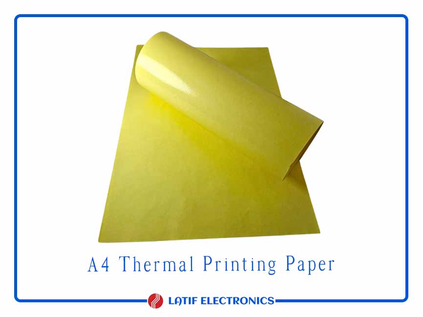
الوصف:
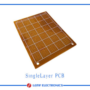
ورق النقل الحراري A4 لطباعة لوحات الدوائر المطبوعة هو ورق مطلي خصيصًا، مصمم لنقل أنماط الدوائر المطبوعة من طابعة ليزر إلى لوح مُغطى بالنحاس. يوفر هذا الورق إطلاقًا سلسًا للحبر عند تسخينه، مما يسمح بإعادة إنتاج آثار لوحات الدوائر المطبوعة بدقة للنقش. وهو مناسب للوحات الدوائر أحادية أو ثنائية الجانب، ويُستخدم عادةً في تصنيع لوحات الدوائر المطبوعة ذاتيًا أو في النماذج الأولية.
خطوات الاستخدام:
- تصميم الدائرة:
أنشئ مخطط لوحة الدوائر المطبوعة باستخدام برامج التصميم مثل EasyEDA أو KiCad أو Altium. اطبع المخطط المعكوس باستخدام طابعة ليزر (وليس طابعة نفث الحبر) على الجانب اللامع من ورق النقل الحراري.
- تحضير لوح النحاس:
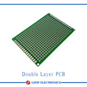
قص اللوح المُغطى بالنحاس بالحجم المطلوب. نظف السطح بورق صنفرة ناعم أو صوف فولاذي، ثم امسحه بالكحول لإزالة الشحوم والأكسدة.
- نقل الحبر:
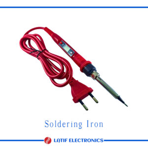
ضع الجانب المطبوع من ورق النقل الحراري على السطح النحاسي. سخّن باستخدام مكواة ملابس أو آلة تغليف على درجة حرارة تتراوح بين 150 و180 درجة مئوية لمدة 3-5 دقائق، مع الضغط بقوة وبشكل متساوٍ.
- التبريد والنقع:اترك اللوح يبرد، ثم انقعه في ماء دافئ لبضع دقائق حتى يلين. انزع الورق أو افركه برفق، مع ترك الحبر ملتصقًا بالنحاس.
- فحص النمط:تحقق من وجود أي كسور أو مناطق ناقصة. أصلح أي عيوب باستخدام قلم تحديد دائم ذي رأس رفيع.
- نقش اللوح:اغمر اللوح في محلول نقش كلوريد الحديديك أو بيرسلفات الأمونيوم حتى تتم إزالة جميع أجزاء النحاس المكشوفة.
- التنظيف والثقب:اشطف اللوح بالماء، وأزل الحبر باستخدام الأسيتون أو الكحول، وثقب ثقوب المكونات حسب الحاجة.
8. اللمسة النهائية: اختياريًا، يُمكن طلاء المسارات بالقصدير أو طلائها لمنع الأكسدة وتحسين قابلية اللحام.
A4 thermal transfer paper circuit board PCB print paper
Description:
A4 thermal transfer paper for PCB printing is a special coated paper designed to transfer printed circuit patterns from a laser printer onto a copper-clad board. It provides smooth toner release when heated, allowing accurate reproduction of PCB traces for etching. It is suitable for single-sided or double-sided circuit boards and is commonly used in DIY or prototype PCB manufacturing.
Steps to Use:
- Design the Circuit:
Create the PCB layout using design software such as EasyEDA, KiCad, or Altium. Print the mirrored layout using a laser printer (not inkjet) on the glossy side of the thermal transfer paper. - Prepare the Copper Board:
Cut the copper-clad board to the required size. Clean the surface with fine sandpaper or steel wool, then wipe with alcohol to remove grease and oxidation. - Transfer the Toner:
Place the printed side of the thermal transfer paper on the copper surface. Apply heat using a clothes iron or laminator at around 150–180 °C for 3–5 minutes, pressing firmly and evenly. - Cool and Soak:
Allow the board to cool, then soak it in warm water for a few minutes until the paper softens. Gently peel or rub off the paper, leaving the toner firmly attached to the copper. - Inspect the Pattern:
Check the traces for breaks or incomplete areas. Repair any defects using a fine-tip permanent marker. - Etch the Board:
Immerse the board in a ferric chloride or ammonium persulfate etching solution until all exposed copper is removed. - Clean and Drill:
Rinse the board with water, remove the toner using acetone or alcohol, and drill component holes as needed. - Finish:
Optionally tin-plate or coat the tracks to prevent oxidation and improve solderability.

المراجعات
لا توجد مراجعات بعد.