")
الوصف العام
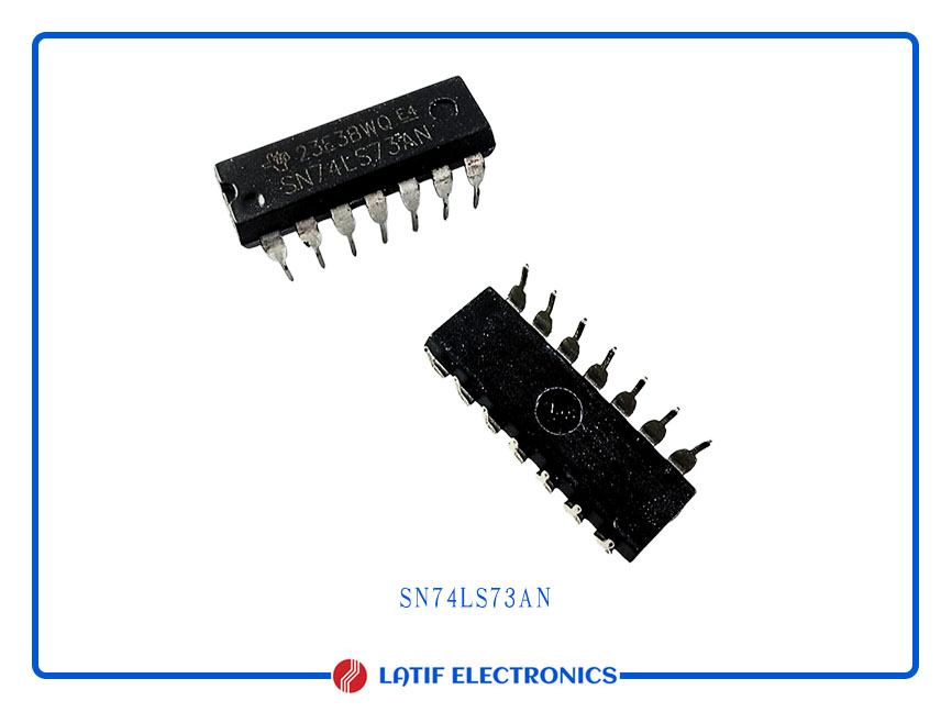
الدارة المتكاملة SN74LS73 هي دارة تحتوي على قلبين (flip-flops) من نوع JK مزدوجة، تعمل بنظام الزناد الحافي عند الحافة السالبة (Negative Edge-Triggered). كل قلب قادر على تخزين بت واحد من المعلومات الثنائية. تعمل هذه الدارة وفق جدول الحقيقة القياسي لنظام JK، حيث يتم تغيير الحالة عند الانتقال من المستوى العالي إلى المنخفض في إشارة الساعة.
طريقة العمل
كل قلب يحتوي على مدخلين للبيانات (J وK)، ومدخل للنبضة (Clock)، ومدخل مسح مباشر (CLR)، ومخرجين متعاكسين (Q و Q̅).
عندما تكون J وK منخفضتين، تبقى الحالة كما هي.
إذا كانت J عالية وK منخفضة، يتم ضبط المخرج (Q=1).
إذا كانت J منخفضة وK عالية، يتم تصفير المخرج (Q=0).
أما إذا كانت J وK كلتاهما عاليتين، فإن المخرج يتناوب بين الحالتين (Toggle) عند كل نبضة سالبة.
آلية الزناد
يعمل هذا المتكامل عند الحافة السالبة لإشارة النبضة، أي أن التغيير في المخرجات يتم فقط أثناء الانتقال من المستوى العالي إلى المنخفض في الإشارة. هذا الأسلوب يضمن تزامناً دقيقاً في الأنظمة الرقمية ويمنع تغيّر الحالة أثناء الفترات الثابتة من نبضة النبضة.
وظيفة المسح (CLR)
مدخل المسح غير المتزامن (CLR) يتجاوز باقي المداخل عندما يكون في الحالة المنخفضة. عند تفعيله (CLR = 0)، يتم تصفير القلب فوراً، حيث يصبح Q = 0 و Q̅ = 1 بغض النظر عن حالة المداخل الأخرى. تُستخدم هذه الخاصية عادةً لتهيئة النظام أو لإعادة الضبط عند حدوث خلل.
التطبيقات
تُستخدم دارة SN74LS73 في العدادات (Counters)، ومقسمات التردد (Frequency Dividers)، وعناصر تخزين البيانات، وأنظمة التحكم التسلسلي. بفضل قدرتها على التبديل (Toggle)، فهي مناسبة لتوليد نبضات تقسيم التردد أو بناء عدادات ثنائية. كما يمكن استخدامها كوحدة تخزين أساسية في الآلات ذات الحالات المحدودة أو شبكات التوقيت.
الخصائص الكهربائية
تنتمي هذه الدارة إلى عائلة TTL منخفضة الاستهلاك (LS TTL) وتعمل بجهد تغذية مقداره 5 فولت ±0.25 فولت.
زمن الانتشار النموذجي يتراوح بين 20 إلى 30 نانوثانية حسب الحمل، والمداخل والمخارج متوافقة مع إشارات منطق TTL القياسية.
ملخص الخصائص
– تحتوي على قلبين JK مستقلين في غلاف واحد
– تعمل عند الحافة السالبة لإشارة النبضة
– مدخل مسح غير متزامن (CLR فعال بالمستوى المنخفض)
– مخرجان متعاكسان (Q و Q̅)
– متوافقة مع منطق TTL
– مناسبة للعدادات، المقسّمات، وأنظمة التحكم التسلسلي
General Description
The SN74LS73 is a dual JK flip-flop IC with clear inputs and negative-edge triggering. It contains two independent JK bistable multivibrators, each capable of storing one bit of binary information. Each flip-flop operates according to the standard JK truth table, with outputs that change state on the falling (negative-going) edge of the clock pulse.
Functional Operation
Each flip-flop features two data inputs (J and K), a clock input, a direct clear (CLR) input, and two complementary outputs (Q and Q̅). When both J and K are low, the output remains unchanged. When J is high and K is low, the flip-flop sets (Q = 1). When J is low and K is high, it resets (Q = 0). When both J and K are high simultaneously, the output toggles state on each clock pulse.
Triggering Mechanism
This device is designed for negative-edge triggering, meaning state changes occur only during the transition of the clock signal from high to low. This ensures precise timing control and synchronization in sequential logic systems, preventing output changes during the stable portions of the clock signal.
Clear Function
The asynchronous clear input overrides the clock and data inputs when activated (low). When CLR is low, the corresponding flip-flop is immediately reset, forcing Q = 0 and Q̅ = 1 regardless of other inputs. This allows external control for initialization or emergency reset conditions in digital systems.
Applications
SN74LS73 devices are widely used in counters, frequency dividers, data storage elements, and sequential control logic. Their toggling capability makes them suitable for building binary counters and divide-by-two circuits. They also serve as basic memory elements in finite state machines and timing networks.
Electrical Characteristics
Operating within the standard LS TTL family, the SN74LS73 requires a single 5V ±0.25V supply and provides typical fan-out compatible with other LS logic devices. Propagation delays are in the range of 20–30 ns, depending on load. Inputs are TTL-compatible, and outputs are designed to drive standard logic-level loads.
Summary of Features
– Two independent JK flip-flops per package
– Negative-edge clock triggering
– Asynchronous clear input (active low)
– Complementary outputs (Q and Q̅)
– TTL-compatible logic levels
– Ideal for counters, dividers, and sequential logic systems
Click here Datasheet: SN54LS73A

المراجعات
لا توجد مراجعات بعد.